Different Types of HDI PCB Constructions
Types of HDI PCB Constructions
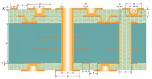
Several different types of HDI PCB constructions are available, some more advanced than others. The two most common are 1+N and 2+N+2. Both offer advantages for increased circuit density and are used in high-performance electronic devices. The 2+N+2 structure is more advanced and allows for greater miniaturization and higher connection counts than the 1+N design.
The 2+N+2 structure uses both standard PCB layers and HDI layers to increase the number of connections per board. Its advantages include a smaller form factor, improved signal transmission and lower costs. In addition, the use of micro vias and via-in-pad technology allows more components to be placed on the PCB, resulting in a more dense layout. The use of laser drilling also enables the vias to be sized to below the maximum limit for mechanical drilling.
These features also help improve the signal integrity of a circuit board due to shorter signal paths. These benefits make hdi pcb suitable for applications that require compactness, reliability and high performance. The PCBs can be fabricated using a variety of materials including FR4, metal or fiberglass, and can be finished with various surface coatings such as ENIG, HASL, immersion tin or gold.
Different Types of HDI PCB Constructions
In order to produce a high-density HDI printed circuit board, the manufacturers need to have the right equipment and processes. This includes laser drills, plugging, laser direct imaging and sequential lamination cycles. The higher the number of layers in a PCB, the more complex and expensive it is to manufacture. In addition, the thinner lines, tighter spacing and annular rings of HDI PCBs require specialized photo tools and clean rooms for fabrication.
Another factor in the cost of HDI PCBs is the amount of time it takes to develop a successful design. This can be a significant obstacle for small projects, especially when the project requires quick turnaround. This is why it’s important to work with a design engineer who can deliver fast and accurate HDI layouts.
A good design will minimize the need for rework and repair by allowing for a better distribution of power and signals throughout the circuit board. This will also reduce the total power consumption of the device. In addition, a good design will have sufficient clearance between the pads and traces to prevent shorting. It is crucial to ensure that your design complies with the manufacturer’s DFM guidelines.
It’s essential to check the manufacturer’s capabilities before embarking on an HDI design. Some manufacturers are only capable of producing a basic 1+N HDI board, while others can support the more advanced 2+N+2 structures. A thorough verification process can save time and money in the long run by avoiding production delays. It’s also necessary to avoid unnecessary features such as staggered vias and Extra-Large Inner Connects (ELIC) unless absolutely required. Keeping these limitations in mind can make a significant difference in the final cost of your circuit board.